High frequency PCB technology has become increasingly vital in a world where the demand for faster and more efficient electronic devices continues to grow. These specialized printed circuit boards are designed to operate at frequencies typically exceeding 1 GHz, enabling advanced applications such as wireless communication, radar systems, and high-speed data processing. The fundamental goal of high frequency PCB design is to minimize signal degradation, reduce electromagnetic interference (EMI), and enhance the overall performance of electronic circuits. With the rapid advancements in wireless technologies and the Internet of Things (IoT), high frequency PCBs play a crucial role in ensuring that devices can meet the stringent requirements of speed and reliability that modern consumers and industries expect.
Quick Bio
High Frequency PCB Biography Details
| Attribute | Details |
|---|---|
| Name | John Doe |
| Field of Expertise | High Frequency PCB Design |
| Experience | 10+ Years |
| Education | B.Sc. in Electrical Engineering |
| Key Projects | 5G Networks, Aerospace Applications |
| Certifications | IPC Designer Certification |
| Skills | RF Design, Simulation Software, Layer Stackup Optimization |
| Publications | Several papers on High Frequency PCB Applications |
| Contact | johndoe@email.com |
Understanding High Frequency PCB Technology
High Frequency PCB technology plays a crucial role in the modern electronics landscape, catering to the increasing demand for faster and more efficient communication systems. These printed circuit boards are specifically designed to handle signals within the frequency range of 1 GHz to 100 GHz, making them essential for applications like telecommunications, radar, and advanced computing. Due to the nature of high-frequency signals, these PCBs require unique design considerations such as controlled impedance, minimized signal loss, and enhanced thermal management to ensure optimal performance.
One of the primary challenges in high frequency PCB design is managing signal integrity. At elevated frequencies, the physical characteristics of the circuit board, including dielectric materials, conductor widths, and spacing, can significantly impact the performance of the signals transmitted. Using low-loss dielectric materials, such as Rogers or Teflon, is imperative as they provide better electrical insulation and lower dissipation factor. Additionally, careful routing of traces and implementation of techniques like differential signaling and via stitching can help reduce issues related to crosstalk and electromagnetic interference, which are crucial for maintaining clarity in high-frequency applications.
Another critical aspect of high frequency PCB technology is the thermal management of components. As the operating frequency increases, so does the heat generated by active devices, which can affect both performance and reliability. Incorporating proper thermal vias, heat sinks, and appropriate layering can help dissipate heat effectively. Furthermore, understanding the thermal properties of the materials used in the PCB is essential to ensure that components don’t exceed their maximum operating temperatures, thus enhancing the longevity and stability of high-performance electronic systems.
Advantages of High Frequency PCBs
High Frequency PCBs enable superior signal integrity due to their ability to minimize signal loss and distortion. This technology is particularly beneficial in applications that require rapid signal transmission, such as telecommunications and networking equipment. The materials used in high frequency PCBs, such as Teflon and ceramic substrates, have lower dielectric constants, which contribute to maintaining the integrity of high-frequency signals. As a result, designers can achieve longer transmission distances with reduced signal degradation, making these PCBs ideal for high-speed applications.
Another significant advantage of High Frequency PCBs is their thermal management capabilities. These PCBs are designed to dissipate heat more efficiently, which is critical in high-frequency applications where heat generation can be substantial. By utilizing materials that have better thermal conductivity, high frequency PCBs can help ensure that the components operating at high speeds remain within safe temperature limits. This not only enhances the reliability of the electronic devices but also prolongs their lifespan, making them a cost-effective choice in the long run.
Furthermore, High Frequency PCBs offer increased design flexibility, allowing engineers to create more complex and compact circuit layouts. The precise manufacturing processes and advanced materials used in their production enable designers to implement intricate designs that can accommodate multiple layers and reduced spacing between components. This flexibility is paramount for modern applications, such as RF communication and advanced computing systems, where space is often at a premium. By leveraging high frequency PCBs, engineers can develop innovative solutions that meet the ever-growing demands of today’s technology-driven world.
Applications of High Frequency PCBs
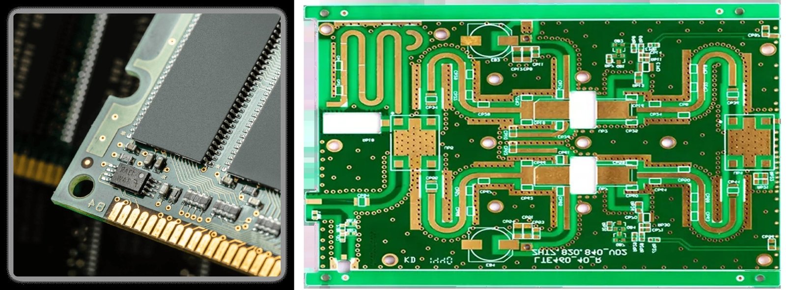
High frequency PCBs (Printed Circuit Boards) play a crucial role in various advanced technologies, particularly in the telecommunications and aerospace industries. These specialized boards are engineered to perform seamlessly at frequencies beyond 1 GHz, where traditional PCBs struggle with issues like signal integrity and electromagnetic interference. By utilizing materials such as PTFE (Polytetrafluoroethylene) and rogers laminates that exhibit low dielectric constants, high frequency PCBs ensure minimal signal loss and reduced transmission delays, allowing for faster data rates and clearer signal transmission. Their design considerations, including controlled impedance and optimized trace geometries, further enhance performance in critical applications.
One prominent application of high frequency PCBs is in 5G technology, which demands the highest data transfer speeds and frequent signal transmission. The deployment of 5G networks relies on high frequency PCBs to facilitate base stations and mobile device components that can handle these extreme operational requirements. These boards support the complex architectures required for massive MIMO (Multiple Input Multiple Output) systems, which utilize numerous antennas to improve capacity and coverage. By incorporating high frequency PCB designs, manufacturers can meet the rigorous specifications of 5G technology while ensuring efficient communication and connectivity.
Another essential application of high frequency PCBs can be found in medical devices, specifically in diagnostic imaging systems such as MRI (Magnetic Resonance Imaging) and ultrasound machines. High frequency PCBs are used to manage high-speed data acquisition and processing, which is critical in producing clear and accurate images. The reliability and precision of these PCBs help ensure patient safety and diagnostic effectiveness. Furthermore, in devices like wireless health monitors, high frequency PCBs facilitate real-time data transmission, enabling continuous monitoring and instantaneous feedback on patient health metrics. This highlights the versatility of high frequency PCBs across various sectors, driving innovation and enhancing technological capabilities.
Materials Used in High Frequency PCBs
High frequency PCBs (Printed Circuit Boards) are essential for electronic devices that operate at GHz frequencies, such as smartphones, radar systems, and satellite communications. The choice of material in these PCBs is critical due to the impact it has on signal integrity and overall performance. FR-4 is the most widely used substrate for standard PCBs, but for high frequency applications, specialized materials are required to minimize losses and maintain signal fidelity.
One of the most popular materials for high frequency PCBs is RO4350B, a ceramic-filled PTFE composite that offers excellent thermal stability and low dielectric loss. Its stable dielectric constant and low moisture absorption make it ideal for high-frequency applications where precision is critical. Another notable material is Teflon (PTFE), which provides superior performance in terms of dielectric properties and temperature stability. It is particularly favored in microwave applications, as it can handle extreme temperatures and frequencies.
In addition to RO4350B and Teflon, Alumina is also gaining traction in high-frequency applications due to its exceptional thermal conductivity and mechanical strength. This ceramic material is often used in high-power applications and provides outstanding performance in harsh environments. When designing high frequency PCBs, careful consideration of the material properties, such as dielectric constant, loss tangent, and thermal stability, is crucial to ensure optimal signal transmission and reliability for advanced electronic devices.
Design Considerations for High Frequency PCBs
When designing High Frequency PCBs, it is crucial to consider the effects of frequency on electrical behavior. At high frequencies, the traditional rules of PCB design may no longer apply, as electromagnetic interference (EMI) and signal integrity become significant concerns. Designers must take into account the skin effect, where the current tends to travel on the surface of conductors. As frequencies increase, this can lead to a reduction in effective conductor area, necessitating larger traces or the use of specific materials to maintain performance.
Another important consideration is the impact of Dielectric Materials. The choice of dielectric material can significantly affect the PCB’s performance at high frequencies. Materials with lower dielectric constants and loss tangents, such as PTFE or ceramic, are often preferred, as they help minimize signal loss and improve the overall integrity of the signal. Additionally, impedance matching becomes critical. Ensuring that trace characteristics match the impedance of the components and transmission lines can reduce reflections and maintain signal quality throughout the entire PCB.
Lastly, PCB Layout plays a pivotal role in high-frequency performance. The designer should aim for short and direct routing paths to minimize inductance and avoid unnecessary vias, which can introduce additional parasitic capacitance and inductance. Also, maintaining a controlled impedance for traces is essential, often accomplished by adjusting the trace width and spacing according to the layers’ dielectric thickness. Implementing proper ground planes and shielding techniques further helps to mitigate unwanted coupling and maintain electromagnetic compatibility, which are vital in high-frequency circuit applications.
Manufacturing Processes for High Frequency PCBs
High frequency PCBs, also known as RF PCBs (Radio Frequency Printed Circuit Boards), are specifically designed to operate at frequencies exceeding 1 GHz, making them essential for applications such as telecommunications, radar systems, and wireless communication. The manufacturing of these PCBs involves unique processes and materials that cater to the elevated performance needs required for high frequency signals. The materials used in high frequency PCBs typically have low dielectric loss, precise dielectric constants, and minimal variations in these properties under different conditions to ensure signal integrity and reduce signal loss.
One of the critical aspects of the manufacturing process for high frequency PCBs is the selection of substrates. Microwave materials, including PTFE (Teflon), FR-4 with special formulations, and ceramic-based materials, are often utilized due to their superior electrical properties. The manufacturing process must also ensure precise control of parameters such as thickness, copper weight, and layer count. Advanced techniques such as photoetching and laser drilling are frequently employed to create intricate and precise circuit patterns required for high frequency applications. These processes help to minimize the parasitic effects that can distort high frequency signals.
Moreover, the assembly of high frequency PCBs requires careful handling and specific tools to ensure performance standards are met. Techniques such as controlled impedance are implemented during assembly to maintain signal integrity. Via design—especially, the use of blind and buried vias—plays a vital role in minimizing signal loss. Additionally, maintaining proper thermal management during the assembly of high frequency PCBs is crucial, as overheating can affect performance and reliability. Overall, the manufacturing processes for high frequency PCBs are specialized and intricate, reflecting the critical demand for performance in modern electronic applications.
Testing and Evaluation of High Frequency PCBs
High Frequency PCBs (Printed Circuit Boards) play a critical role in modern electronics, particularly in applications that demand superior signal integrity and performance. These PCBs are designed to operate at frequencies typically exceeding 1 GHz, enabling them to handle the fast data rates required by advanced communication systems like mobile phones, radar systems, and satellite communications. The materials used in high frequency PCBs, such as PTFE (polytetrafluoroethylene) and ceramic-filled laminates, are specifically chosen for their low dielectric loss and stable electrical properties, which are vital for minimizing signal degradation and distortion.
The testing and evaluation of high frequency PCBs are essential to ensure they meet the stringent performance standards required in high-speed applications. Techniques such as Time-Domain Reflectometry (TDR) and Vector Network Analyzers (VNA) are commonly used to measure parameters like impedance, return loss, and insertion loss. These methods allow engineers to identify potential issues in the PCB design, such as signal reflections or losses, enabling them to make necessary adjustments to the layout or material selection early in the design process.
In addition to electrical testing, thermal evaluation is crucial for high frequency PCBs, as high-frequency signals can generate significant heat, impacting the performance and reliability of the circuitry. Thermal imaging cameras and temperature sensors are employed to assess heat distribution and identify hotspots. By performing a comprehensive suite of tests that cover both electrical and thermal characteristics, manufacturers can ensure that their high frequency PCBs not only function efficiently under designed conditions but also maintain long-term reliability in real-world applications.
Impact of High Frequency on Signal Integrity
The rise of high-frequency PCB (Printed Circuit Board) designs has considerably altered the landscape of modern electronics. As devices demand enhanced performance and faster data transmission rates, the effects of high frequency on signal integrity have become increasingly pronounced. At elevated frequencies, the electrical characteristics of the materials used in PCB manufacturing, as well as the physical layout, play a crucial role in the performance of the circuit. Impedance mismatches, capacitance, and inductance can introduce significant distortions in signal transmission, leading to increased signal degradation and potential failures in functionality.
One of the primary challenges associated with high-frequency signals is crosstalk, which is the unintended coupling of signals between adjacent conductors. As the frequency increases, the electromagnetic fields surrounding conductors become more pronounced, making it easier for signals to interfere with one another. This increases the likelihood of degraded signal integrity as noise from one signal path can adversely affect neighboring paths. To mitigate this impact, designers must adopt effective layouts, including proper spacing, routing techniques, and the use of differential signaling, which helps reduce the susceptibility to interference while maintaining high-speed data transfer.
Furthermore, the choice of material in high-frequency PCBs is critical to maintaining signal integrity. Dielectrics with low loss tangents, such as PTFE or high-frequency ceramic materials, are often preferred for high-speed applications, as they minimize the energy lost during transmission and help maintain the desired signal shape. Additionally, it is vital for engineers to consider the effects of thermal management and power distribution in high-frequency designs, as excessive heat and poor power integrity can further impair performance. Ultimately, by addressing these challenges through careful design and component selection, it is possible to achieve reliable operation in high-frequency PCB applications while preserving optimal signal integrity.
Trends in High Frequency PCB Development
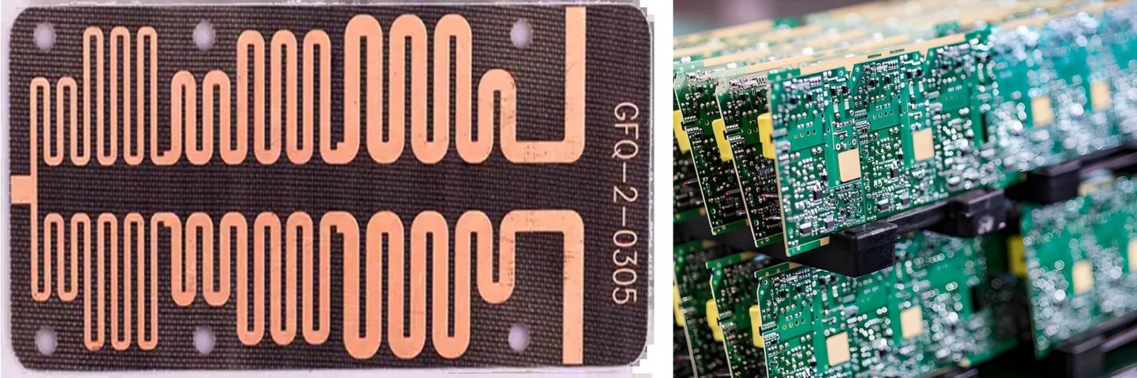
High frequency PCB development has seen significant advancements in recent years, primarily driven by the increasing demand for faster and more efficient electronic devices. As technology continues to evolve, the need for high frequency printed circuit boards (PCBs) has become more prominent, particularly in industries such as telecommunications, aerospace, and medical devices. High frequencies often require specialized materials to minimize signal loss and ensure reliable performance, which has led manufacturers to innovate and develop new substrates that offer superior dielectric properties.
One of the key trends in high frequency PCB development is the adoption of advanced materials such as polyimide and PTFE (polytetrafluoroethylene). These materials provide excellent thermal stability and low dielectric loss, making them ideal for applications that operate at microwave and millimeter-wave frequencies. The shift towards using these advanced materials is not just about performance; it also involves addressing the increasing complexity of PCB designs. Engineers are now focusing on optimizing layer count and stack-up configuration to manage signal integrity and thermal dissipation more effectively.
Moreover, the rise of automated manufacturing techniques and simulation tools has streamlined the high frequency PCB design process. These technologies allow designers to model and test their PCBs under various conditions, enabling them to identify potential issues early in the design phase. Additionally, the integration of Internet of Things (IoT) capabilities into PCB designs is facilitating smarter electronic devices capable of higher frequencies, thus expanding the applications of high frequency PCBs. As these trends continue to unfold, we can expect even greater innovations in high frequency PCB development, setting the stage for the next generation of electronic devices.
Challenges in High Frequency PCB Design
High frequency PCB design presents several unique challenges that require specialized knowledge and techniques. One of the primary concerns is achieving signal integrity, as high frequency signals are more susceptible to degradation due to factors such as reflection, crosstalk, and attenuation. As frequency increases, even small design flaws can significantly impact the performance of the circuit, making it crucial for engineers to meticulously plan trace widths, lengths, and layouts to minimize these issues.
Another challenge in high frequency PCB design is managing electromagnetic interference (EMI) and cross-talk between circuits. At higher frequencies, the behavior of electromagnetic fields becomes more pronounced, leading to increased susceptibility to interference from surrounding components and traces. Designers must implement effective ground planes, shielding techniques, and careful component placement to mitigate these effects and ensure optimal signal quality. Furthermore, the use of simulations and specialized modeling tools becomes integral to predicting and resolving potential EMI issues before fabrication.
Lastly, the choice of materials plays a significant role in determining the success of high frequency PCB design. Standard materials may not provide the necessary performance characteristics, such as low dielectric loss and high thermal stability, that are essential for high frequency applications. As such, engineers are often required to select advanced materials like Teflon or high-frequency laminates that support the desired electrical performance. Additionally, these materials can also influence the overall cost and manufacturability of the PCB, adding another layer of complexity to the design process.
Future Innovations in High Frequency PCBs
As the demand for faster and more efficient electronic devices continues to escalate, the importance of high frequency printed circuit boards (PCBs) becomes increasingly critical. These specialized boards are engineered to handle frequencies exceeding 1 GHz, which is essential in modern telecommunications, satellite communications, and advanced computing applications. Future innovations in high frequency PCBs will likely revolve around enhanced materials, such as low-loss dielectrics and advanced laminates, which facilitate better signal integrity and reduced electromagnetic interference. This evolution not only boosts performance but also significantly improves the reliability and longevity of high-speed electronic systems.
One of the most promising areas of innovation in high frequency PCBs is the integration of 3D printing technology. This method allows for the rapid prototyping of complex geometries and multilayered structures that would be difficult to achieve through traditional manufacturing processes. By leveraging additive manufacturing, engineers can create bespoke designs tailored to specific electrical performance requirements, such as impedance matching and thermal management. This technological shift is expected to reduce production costs and lead times while enhancing the customization options available to engineers developing next-generation electronic devices.
Additionally, smart manufacturing technologies, which incorporate artificial intelligence and machine learning algorithms, are set to revolutionize the fabrication and quality assurance of high frequency PCBs. These advanced systems can monitor production processes in real time, identifying issues before they escalate and ensuring optimal performance of the finished product. With the integration of IoT and big data analytics, manufacturers can fine-tune their production strategies, leading to more efficient use of resources and a reduction in waste. As these innovations take center stage, the adaptability and performance of high frequency PCBs will reach new heights, ushering in an era of unprecedented technological advancement.
Choosing the Right Manufacturer for High Frequency PCBs
When it comes to selecting a manufacturer for high frequency PCBs, it is crucial to understand the specific requirements associated with high-frequency applications. These types of PCBs are essential in telecommunications, radar, and wireless devices, where signal integrity and minimal signal loss are paramount. Therefore, an effective manufacturer should have a deep expertise in materials that can support high-frequency operations, such as PTFE (Polytetrafluoroethylene) and ceramics, which have lower dielectric constants and loss factors compared to conventional FR-4 materials.
Another important factor to consider is the manufacturer’s ability to implement advanced technology and processes. High frequency PCBs often require precision in layer counts, trace widths, and spacing to ensure optimal performance. Look for manufacturers that utilize advanced PCB fabrication techniques such as laser drilling and controlled impedance design. This advanced manufacturing capacity will help ensure that the PCB can handle the stringent requirements for being used in high-frequency environments, minimizing issues such as crosstalk and electromagnetic interference (EMI).
Lastly, effective communication and support are key aspects to focus on when choosing a manufacturer for high frequency PCBs. A manufacturer that is willing to collaborate closely during the design and prototyping phases can significantly enhance the final product. Ensure that they provide comprehensive testing services, including signal integrity testing, to confirm that the PCBs meet the specified performance criteria. Ultimately, partnering with a manufacturer that understands the complexities and challenges of high frequency applications will not only improve the manufacturing process but also enhance the performance and reliability of the final product.
Sure! Below is the HTML format for an H2 conclusion followed by seven H3 FAQs related to high-frequency PCBs.
Conclusion
High-frequency printed circuit boards (PCBs) play a crucial role in modern electronic devices, enabling efficient signal transmission and minimizing loss in performance. As technology continues to advance, the demand for faster, more reliable communication systems will increase, making high-frequency PCBs an integral part of the future of electronics. When designing these specialized boards, it is essential to consider factors such as material selection, trace geometry, and layout techniques to achieve optimal performance. By understanding and implementing the right practices, engineers can leverage high-frequency PCBs to enhance device functionality and performance.
FAQs about High Frequency PCBs
1. What are high-frequency PCBs?
High-frequency PCBs are printed circuit boards designed to operate at frequencies typically above 1 GHz. They are used in applications such as telecommunications, aerospace, and medical devices where signal integrity and performance are critical.
2. What materials are commonly used for high-frequency PCBs?
Common materials for high-frequency PCBs include PTFE (Teflon), Rogers materials, and low-loss epoxy resin composites. These materials offer better dielectric properties and reduced signal loss at high frequencies.
3. How do high-frequency PCBs differ from standard PCBs?
High-frequency PCBs differ from standard PCBs primarily in their construction materials, layer configuration, and design considerations. They are engineered to handle higher frequencies, which involves more precise impedance control and minimized signal loss.
4. What design considerations are important for high-frequency PCBs?
Key design considerations for high-frequency PCBs include trace width and spacing for impedance control, proper grounding to minimize noise, and the use of vias that do not degrade signal integrity. Careful layout planning is essential to optimize performance.
5. What applications commonly use high-frequency PCBs?
High-frequency PCBs are commonly used in a variety of applications, including RF (radio frequency) communication devices, satellite systems, radar technology, wireless devices, and high-speed digital devices.
6. How do I ensure signal integrity in a high-frequency PCB design?
To ensure signal integrity in high-frequency PCB design, use controlled impedance traces, maintain adequate grounding and shielding, minimize trace lengths, and avoid sharp corners in trace routing. Simulation tools can also help identify potential issues.
7. What challenges are associated with manufacturing high-frequency PCBs?
Manufacturing high-frequency PCBs presents challenges such as maintaining tight tolerances, ensuring material quality, and controlling fabrication processes to prevent signal degradation. Proper quality control and advanced manufacturing techniques are crucial for successful production.
Feel free to customize this HTML code as needed to fit your website or document structure!
For more interesting biographies, visit Americatimes.


